

pushing the boundary of high precision metal manufacturing with Electroforming

 Electroforming is a metal forming process by means of electrodeposition, similar to Electroplating and Electrorefining. The electrodeposition process takes place in an electrolytic bath and involves two electrodes (an anode and a cathode) and an electrolytic solution. The mandrel is placed in the bath and the electrodes pass a DC through the solution. The DC converts metallic ions into atoms that are continuously deposited on the conductive areas of the mandrel until the desired metal thickness has been achieved.
Compared to other traditional metal forming technologies, for example casting, forging, stamping, or deep drawing, Electroforming can deliver mass volume at superior accuracy and extreme design complexity, due to the fact that it can replicate the shape of the mandrel at extreme accuracy.
Electroforming is also an additive manufacturing process specialized for the production of high precision metal parts. Its uniqueness is that you can grow metal parts atom by atom, providing extreme accuracy and high aspect ratios. Typical precision of a electroformed part goes down to 1 to 2 μm, which is beyond what most other manufacturing technologies can reach.
Veco, as the world leader and largest independent supplier of Electroforming, has been moving the industry forward, with unparalleled experience of Electroforming, advanced lithography technology, and accumulated knowledge of metallurgy. Veco’s unique Advanced Lithographic Electroforming, also referred to as Advanced Photo Electroforming, is predominantly done with nickel, followed by palladium nickel or copper, depending on specific demand (learn more about materials).
Veco’s Advanced Electroforming process is a unique combination of unparalleled industry experience of Electroforming, advanced lithography technology, and accumulated knowledge of metallurgy. It comprises 6 steps.
1) Cleaning
A metal sheet substrate is cleaned and degreased.
2) Coating
The cleaned metal ‘blank’ is then coated with a light-sensitive photoresist.
3) Exposing
The metal sheet is then exposed to ultra-violet light, which hardens the photoresist.
4) Developing
After the image is transferred by UV exposure the substrate is developed, rinsed and dried.
5) Deposition
An electrolytic bath is used to deposit metal onto the patterned surface.
6) Harvesting
The electroformed part can be harvested from the mandrel, once the material is plated in the desired thickness.
7) Inspection
Full inspection by experts.
(1) Plating Defined Electroforming: the Overgrowth Method
Plating defined electroforming is also referred to as an overgrowth method.
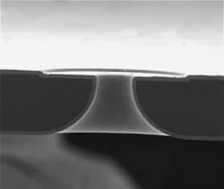
Fig. cross section of an overgrowth product.
It uses a thin photoresist pattern to shield parts of the conductive substrate. A light-sensitive coating is applied to the conductive surface, and it will polymerize where it is exposed to UV light. Metal grows over the photoresist and the thickness of the product exceeds the thickness of the photoresist, hence the process is also known as overgrowth. Note that outer corners will round off during growth, while inner corners will be sharp.
The process is mainly used to make sheets with small conical orifice s for filtration and (ink)jetting.
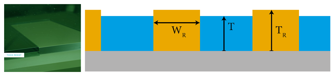
(2) Photo Defined Electroforming: the Thick Resist Method
Photo defined electroforming is also called the thick resist method.

Fig. cross section of a hole made by thick resist
In some cases, it is desired to make the product thicker. This is when the thick resist method is applied. A thick pattern of photoresist is used during photo defined growth, such that the thickness of the product does not exceed the thickness of the photoresist.
Aspect ratios up to 1 can generally be achieved with ease. The exact limits depend on the size and geometry of the products .
(3) Surface Replication with Electroforming
The electroforming process allows for extremely precise duplication of the mandrel.

Fig. Example of surface replication by Electroforming
The high resolution of the conductive patterned substrate allows finer geometries, tighter tolerances, and superior edge definition. This results in perfect process control, high-quality production and very high repeatability.
Electroforming is therefore perfectly suitable for high precision surface replication at low cost and in high volumes.

1) Cleaning
A metal sheet substrate is cleaned and degreased.
2) Coating
The substrate is coated in a light-sensitive coating/photoresist.
3) Exposing
The substrate is exposed to ultraviolet (UV) laser direct imaging (LDI), whereby the CAD part pattern is projected and transferred onto its surface. The resulting patterned surface is split into conductive areas and non-conductive areas by the photoresist material hardening in the latter.
4) Developing
The patterned substrate is developed, meaning the unexposed photoresist is removed to expose the conductive areas. It is then rinsed and dried. The patterned substrate is from here on referred to as the mandrel (part model).
5) Electrodeposition
The electrodeposition process takes place in an electrolytic bath and involves two electrodes (an anode and a cathode) and an electrolytic solution. The mandrel is placed in the bath and the electrodes pass a DC through the solution. The DC converts metallic ions into atoms that are continuously deposited on the conductive areas of the mandrel until the desired metal thickness has been achieved.
6) Harvesting
The electroformed part is harvested, or separated, from the mandrel. The electroforming process can be managed in different ways to achieve different product features. For example, if a thin photoresist is used and the metal is allowed to grow over it, resulting in the thickness of the part exceeding that of the photoresist, the outer edges will be rounded and have a bell mouth shape. Alternatively, if a thick photoresist is used and the metal is not allowed to grow over it, resulting in the thickness of the part being less than the thickness of the photoresist, the outer and inner edges will be straight and sharp.
Typical materials we offer for Electroforming are Nickel and Copper. Whereas we have a variety of nickel types available with different material properties:
1) Veco84
2) Sulfamate
3) Meta
4) Hr-Ni
5) PdNi (Biocompatible)
(1) Plating Defined Electroforming: the Overgrowth Method
With Plating Defined Electroforming, metal grows over the photoresist and the thickness of the product (T) exceeds the thickness of the photoresist (TR), hence the process is also known as overgrowth.


(2) Photo Defined Electroforming: the Thick Resist Method
With Photo Defined Electroforming, a thick pattern of photoresist is used during photo defined growth, such that the thickness of the product (T) does not exceed the thickness of the photoresist (TR).
Aspect ratios (TR/ WR) up to 1 can generally be achieved with ease. The exact limits depend on the size and geometry of the products .

(3) Surface replication with Electroforming
With surface replication, positional accuracy is determined by stress in EF material and accuracy of exposure method (For glass tooling and LDI the accuracy is so high that the accuracy in the final product is solely determined by the EF process). Generally, positional accuracy of the LDI/glass tooling is ±0.15‰ and film tooling ±0.25‰.
Feature accuracy of overgrowth is ±2 µm and ±0.75 µm on standard deviation on a 50 µm thick product.
Accuracy of features on photo-defined is generally ±5 µm for LDI/glass tooling and ±10µm for film tooling.
For mm/cm size features, the accuracy drops by ±0.15‰/±0.25‰.
The demand for energy transition is constantly increasing, especially since the Paris Agreement stipulates that the world must become greenhouse gas neutral by the second half of the century to limit the increase of global temperatures to a maximum of 2°C. Solar power plays a very important role in energy transition and climate protection as it affords a drastic reduction in greenhouse gasses, which arise through the burning of fossil-based fuels such as oils, coal and gas.
In this context, accumulated research and effort has been taken to improve the efficiency of solar power. Crystalline silicon (Si) photovoltaic (PV) cells are the most common solar cells used in commercially available solar panels. They have dominated the PV cell market since its early beginnings, around the 1950s, and account for more than 90 percent of it today.
The outlook for higher efficiency in photovoltaic cell manufacturing — from better screens to no screens
A large number of PV cell manufacturing companies and research institutes have been devoted to improving cell efficiency and reducing costs to develop high-efficiency crystalline Si PV cells. An essential step in producing these cells is the metallisation process of creating a grid of very fine lines on the front side of the wafer that conduct the light-generated electrons away from the cell.
This metallisation process is most often undertaken using screen printing technology, whereby conductive paste is forced through the openings of a wire mesh or emulsion screen onto the wafer to form the circuits or contacts. Over the years, efforts to improve the efficiency and precision of PV cell metallisation have led to better screen printing equipment and materials. For example, high-precision stencils have been introduced as an alternative to traditional wire mesh and emulsion screens. Moreover, the development of inkjet printing and 3D metal printing technologies has allowed for the realisation of maskless screen printing.
(1) Screen printing
The screen printing process begins with an Si wafer being placed on a printing table. A screen, usually a wire mesh or emulsion screen, is mounted within a frame and placed over the wafer. This screen blocks certain areas and leaves other areas open. Metal paste, usually silver (Ag), is then dispensed onto the screen using a squeegee so that it is spread uniformly to fill the screen openings. As the squeegee moves across the screen, it pushes the paste through the openings, transferring it onto the wafer.
A grid of conductive circuit lines is deposited this way. These thin and delicate lines, also referred to as fingers, collect and conduct the light-generated electricity from the active regions to larger collecting lines, or busbars, and then to the module’s electrical system.
However, the lines are not as thin as desired, since they block sunlight from reaching active parts of the cell and thus reduce conversion efficiency. To minimise this so-called shadowing effect, efforts have been made to make the lines as narrow as possible as well as taller to maintain the same cross-section for adequate conductivity.

screen printing process illustration
(2) Stencil printing
The stencil printing process was introduced after the screen printing process. The development of high-precision metal manufacturing technologies such as electroforming meant that high-precision stencils became an alternative for achieving achieve finer, taller contacts in PV cell manufacturing. As in screen printing, these stencils, with blocked and open areas, are used to apply paste to the wafer.
Stencil printing overcomes the limitations of screen printing in aspect ratio (i.e. line height/line width), finger width and uniformity. The much finer lines with higher aspect ratio and better durability. All of these in the end lead to much higher yield and lower cost. Lab tests have shown stencil printing as offering a 0.25 percent PV cell efficiency improvement over screen printing.

Electroformed Solar Cell Stencil
(3) Inkjet printing
Inkjet printing is an extremely versatile, non-contact process that involves jetting tiny ink droplets to facilitate direct printing. Besides printing graphics on all kinds of surfaces, industrial inkjet printers today can deposit a wide range of inks with ultra-precise accuracy on various substrates. Thanks to inkjet printing being non-contact and that available inks range from polymers and metal nanoparticles to living cells, inkjet printing has seen a surge of new applications in fields including electronics, life science, PVs and optics.
In PV cell manufacturing, inkjet printing deposits metal paste directly onto the surface of the cell through very miniscule openings of a highly efficient, parallel print head, providing a contactless, maskless printing alternative to conventional screen printing and stencil printing. This dispensing process provides the PV industry with multifaceted benefits over conventional screen printing, such as those outlined below.
Increased efficiency and electricity output
In screen printing, a squeegee is used to push the metal paste through the screen openings and onto the wafer surface. The typical line width is 55–80 μm, resulting in shadowing loss of 7–10 percent. Moreover, lines have a low aspect ratio of c.a. 0.2–0.5.
In inkjet printing, the lines can be made much thinner, exposing a larger semiconductor surface to the sunlight. The lines also have a better aspect ratio, ensuring a larger portion of incoming sunlight is reflected towards the wafer instead of back into the air. These two factors increase efficiency by approximately 1 percent and electricity output.
Reduced metal paste consumption
In screen printing, the wire mesh and emulsion screens are repeatedly used and the openings can gradually get blocked or deform, resulting in lines broadening, becoming irregular and having ragged edges.
In inkjet printing, finer lines with higher aspect ratios and lower striations can be achieved. Moreover, high-speed dispensing using intermittent parallel operation of hundreds of nozzles down to several micron can be flexibly optimised in terms of nozzle number and arrangement. The accuracy and flexibility enable homogeneous line shape, contributing to a 20 percent reduction in metal paste consumption.
Significant throughput potential
Inkjet printing, being non-contact, promises a lower reject rate if used on thinner Si wafers. Also, being inline, it increases throughput significantly over conventional screen printing.
To sum up, the maskless nature of inkjet printing affords a high material utilisation rate, improved output and efficiency, freedom of design and significant throughput potential. Moreover, it can be directly integrated into an existing silicon PV cell production facility, replacing the screen printing process utilised for front-side metal contacts.
How electroforming has empowered the contactless metallisation process
A vital part of the dispensing print head is the high-precision nozzle plate, produced using electroforming, a micro-precision, metal additive manufacturing (AM) process combining lithography and electrodeposition. The nozzle plate is a rectangular, elongated part with miniature holes, through which the metal paste is pressed and deposited via the nozzles onto the PV cell in very thin straight lines.

inkjet nozzle plates gold plated
Another significant advantage of electroforming is reproducibility. The process affords precision of approximately 5 μm. In a plate that has 100 to 200 miniature nozzles in a straight line, each of those nozzles needs to be the correct size, not only on each plate but on every plate and across different batches of the plate. Electroforming guarantees reproducibility, meaning the same drawing and process setup translates to perfectly uniform and reproducible printing results and the exact same product time and time again.
Electroforming can also be used to produce special hole geometries; for example, bell mouth shaped holes not achievable using traditional cutting and drilling processes. These holes can effectively reduce blinding/clogging of the plate/nozzles, thus ensuring exceptional paste release performance.
A final point of note is that plate material resistance is especially important in PV cell production because the metal paste used can be corrosive. Also, the pressure applied to push the paste through the plate makes deformation a potential risk. For these reasons, Veco offers a range of alloys that have highly stable contact resistance and excellent mechanical characteristics, ensuring exceptional printing performance over a longer lifetime.