Electroforming:
additive manufacturing
atom by atom

what is ELectroforming/Photo-Electroforming?

Electroforming is an additive manufacturing process specialized for producing high-precision metal parts. Its uniqueness is that you can grow metal parts atom by atom, providing extreme accuracy and high aspect ratios. (check our design guideline to learn technical possibilities)

Once you’ve discovered the benefits of the technology, a whole new world of opportunities opens up. What if you could produce, atom by atom, stress- and burr-free precision metal parts with micron-scale accuracy? It would give you the opportunity to raise the bar on precision, tolerance, cost-effectiveness, and the capability to withstand higher temperatures.

As the world leader in high-precision manufacturing, Veco is the first in the industry to apply advanced Laser Direct Imaging technology. At Veco nowadays, 90% to 95% of our photolithography process is done by Laser Direct Imaging. The combination of LDI and our leading EF technology has enabled us to further push the boundaries of the industry, providing our customers with high-precision metal components of higher quality, at lower cost, and with a quicker turnaround.

electroforming: key features

conical hole shape
unique hole configuration
besides straight holes, it is also possible to achieve special bell mouth hole shape
thickness range
thickness range 5 – 1200 micron
feature size
feature size down to 2 micron
tight tolerance
tight tolerance down to +- 1 micron
design flexibility
complex shapes and design configurations with different materials
3D structures
complex 3D structures can be achieved by growing additional layers in different directions
high quality
burr-free, stress-free components with ultra smooth surface and clear edges
cost efficiency
highly cost efficient from prototyping to industrial scale mass production

Electroforming process: combining photolithography and electrodeposition

cleaning

The metal substrate will first be cleaned
and degreased.

coating

The cleaned metal ‘blank’ is then coated with a light-sensitive coating/photoresist.

exposing

The metal sheet is then exposed to ultra-violet light, which hardens the photoresist.

We use the LDI (Laser Direct Imaging) technology which is highly accurate. Also, with an LDI, photomasks become redundant, which significantly reduces costs and decreases lead time.

developing

After the image is transferred by UV exposure the substrate is developed, rinsed and dried.

deposition

An electrolytic bath is used to deposit metal onto the patterned surface.

The electro-deposition process involves an electrolytic solution, two electrodes, and a DC current. The DC of electricity is passed through the solution, transferring metal ions onto the cathodic surface through a continuous deposit. Therefore, the material can be built up on microscale accuracy: atom by atom.

harvesting

The electroformed part can be harvested from the mandrel, once the material is plated in the desired thickness.

more about Electroforming process: watch the full video

explore what electroforming can bring to your next project
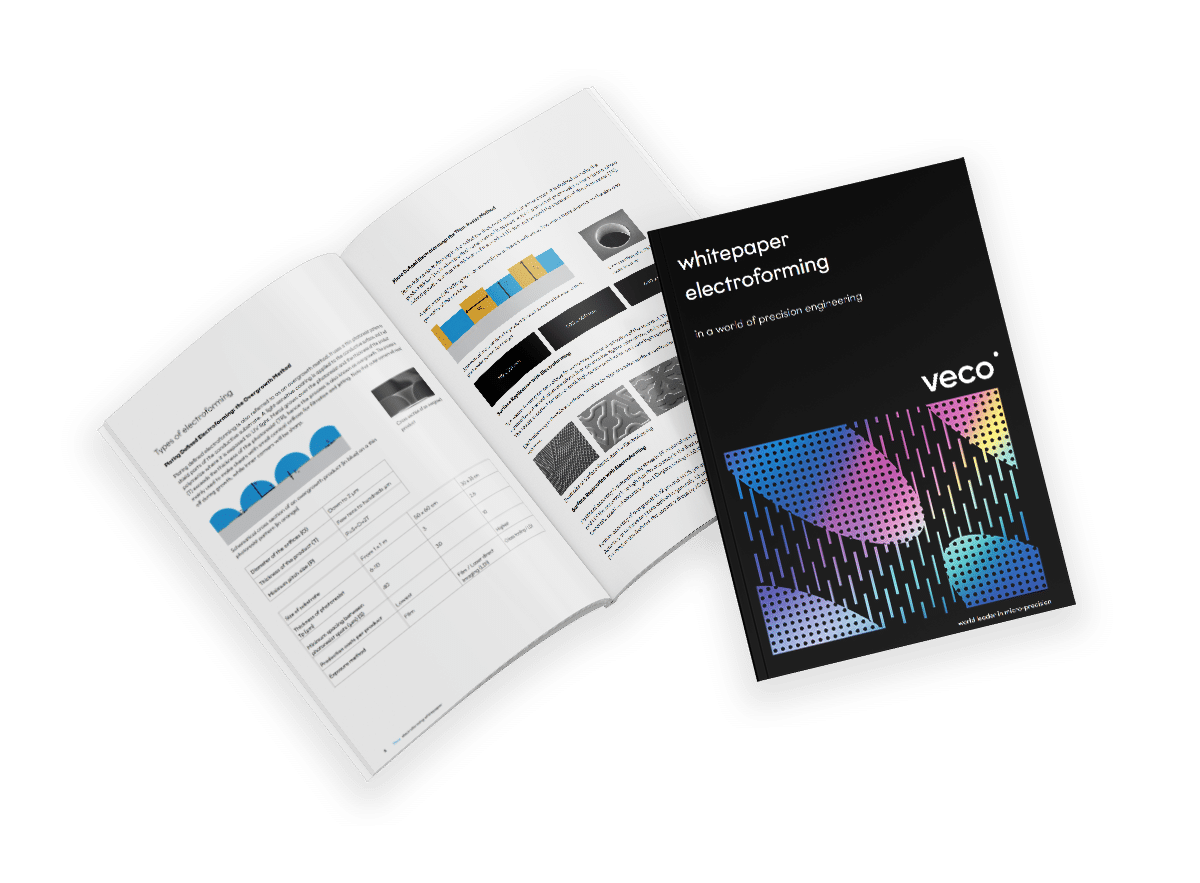
download whitepaper to learn about possibilities of our technology and how it can benefit your next innovation
download whitepaper